
Applying memory design technology from
Osaka to the world
Would you like to join the team too?
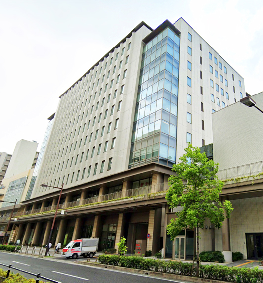
Would you like to design memory IC chips? Our office building is located within a 2-minutes walk from Japan Rail Amagasaki Station.
Even fresh graduates and inexperienced individuals can learn memory IC design from scratch - aiming to be a first-class designer/engineer.
Although Zentel is headquartered in Japan, foreign nationals and international students can work globally in collaboration with subsidiaries in Taiwan, China and the United States.
Make the most of your career - we are also looking for mid-career hires of experienced professionals.
Japan became a DRAM world leader in the 1980s. However, when South Korea took over the majority of this industry in the 1990s, major semiconductor brands withdrew from DRAM business one by one and now there is no major DRAM manufacturer left with Japanese capital.
Is there no future in DRAM business after all? It still is. From a global perspective Taiwan is the next big player after Korean and US majors and over recent years China has been investing significant capital in DRAM manufacturing and design and first class designers receive favorable rewards worldwide.
As a young person we could educate you in this technology that originated from a major Japanese manufacturer and if you are an experienced professional you are also welcome to join this powerful team.
Here at the Zentel Japan R&D center in Osaka we are looking forward to find new talented members for our team of friends that will make advanced memory chip design and production happening.
New graduate・Overview of recruiting inexperienced people
Occupation
Memory (DRAM) designer (circuit / layout design, design verification)
Recruitment personnel
5 people / year
Qualification
Those who have completed education at a bachelor level or higher in science and engineering
Japanese ability to work in Japan
treatment
Annual salary system based on the starting salary of a major manufacturer
There is a bonus system according to the performance of the previous year
Stock option system available
Hiring process
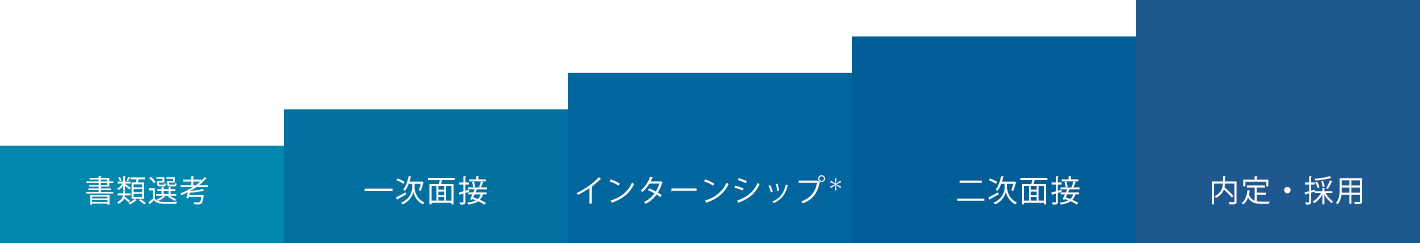
* Internships can be substituted during the trial period
Mid-career recruitment overview
Occupation
Memory (DRAM) designer (circuit / layout design, design verification)
Recruitment personnel
Some people
Qualification
Work experience in LSI (especially memory) circuit / layout design
treatment
Annual salary system
Determined in consideration of experience content / level and treatment of previous job
There is a bonus system according to the performance of the previous year
Stock option system available
Hiring process
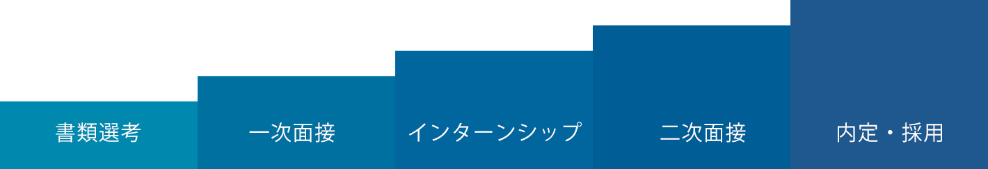
* Internships can be substituted during the trial period
Tokyo head office
There are no hiring plans at this time.